Source: Internet Compilation • Author: Anonymous
The push for higher performance, miniaturization, and operation at higher frequencies is challenging the limits of two key antenna-connected components in wireless systems: the power amplifier (PA) and the low-noise amplifier (LNA). Efforts to make 5G a reality, as well as the use of PAs and LNAs in VSAT terminals, microwave radio links, and phased array radar systems, have contributed to this shift.
The requirements for these applications include lower noise (for LNAs) and higher energy efficiency (for PAs), as well as operation at higher frequencies up to or above 10 GHz. To meet these growing demands, LNA and PA manufacturers are shifting from traditional all-silicon processes to gallium arsenide (GaAs) for LNAs and gallium nitride (GaN) for PAs.
This article will introduce the roles and requirements of LNAs and PAs, as well as their main characteristics, followed by typical GaAs and GaN devices and considerations to keep in mind when designing with these devices.
The Sensitive Role of the LNA
The role of the LNA is to capture extremely weak and uncertain signals from the antenna, which are typically in the microvolt range or below -100 dBm, and then amplify these signals to a more useful level, usually around 0.5 to 1 V (Figure 1). Specifically, in a 50 Ω system, 10 μV corresponds to -87 dBm, and 100 μV equals -67 dBm.
While it is easy to achieve such gain with modern electronics, the situation becomes far more complicated when the LNA introduces various types of noise into the weak input signals. The amplification advantage of the LNA can be completely lost in such noise.
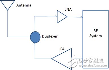
Figure 1: The low-noise amplifier (LNA) in the receive path and the power amplifier (PA) in the transmit path are connected to the antenna via a duplexer, which separates the two signals and prevents the relatively strong PA output from overloading the sensitive LNA input. (Image source: Digi-Key Electronics)
It should be noted that the LNA operates in a world full of uncertainties. As the front end of the transceiver channel, the LNA must be able to capture and amplify low-voltage signals with extremely low power within the relevant bandwidth, as well as the associated random noise caused by the antenna. In signal theory, this situation is called the unknown signal/unknown noise problem, which is the most difficult part of all signal processing problems.
The main parameters of the LNA are noise figure (NF), gain, and linearity. Noise comes from thermal sources and other noise sources, with typical NF values ranging from 0.5 to 1.5 dB. The typical gain of a single-stage amplifier is between 10 and 20 dB. Some designs use a cascaded amplifier with a higher gain stage following a low-gain, low-NF stage; this design may achieve a higher NF, but once the initial signal has been "amplified," this becomes less important. (For more details on LNAs, noise, and RF receivers, please refer to the article "Low-Noise Amplifiers Can Maximize Receiver Sensitivity" in TechZone.)
Another issue with LNAs is nonlinearity, as synthesized harmonics and intermodulation distortion can degrade the quality of the received signal, making signal demodulation and decoding more difficult even when the bit error rate (BER) is quite low. The third-order intercept point (IP3) is commonly used as a characterization parameter for linearity, correlating the nonlinear products caused by third-order nonlinear terms with the signal amplified in a linear manner; the higher the IP3 value, the better the linearity of the amplifier's performance.
Power consumption and energy efficiency are usually not a primary concern in LNAs. By nature, the vast majority of LNAs are devices with relatively low power consumption and current draw between 10 and 100 mA. They provide voltage gain to the next stage but do not deliver power to the load. Moreover, only one or two LNAs are used in the system (the latter is often used in multi-functional antenna designs for interfaces such as Wi-Fi and 5G), so the energy savings from low-power LNAs are minimal.
Apart from operating frequency and bandwidth, various LNAs are relatively similar in functionality. Some LNAs also have gain control capabilities, enabling them to handle a wide dynamic range of input signals without overload or saturation. In mobile applications with a wide range of channel losses from base stations to mobile phones, encountering such a wide range of input signal strengths is common, even in single-connection loops.
The routing of the input signal to the LNA and the output signal from it is as important as the specifications of the component itself. Therefore, designers must use sophisticated modeling and layout tools to realize the full potential performance of the LNA. Poor layout or impedance matching can easily degrade high-quality components, so it is essential to use the Smith chart provided by the supplier (see "Smith Chart: Still a Crucial 'Ancient' Graphic Tool in RF Design") and reliable circuit models that support simulation and analysis software.
For these reasons, almost all suppliers of high-performance LNAs operating in the GHz range provide evaluation boards or verified printed circuit board layouts, as every aspect of the test setup is crucial, including layout, connectors, grounding, bypassing, and power supply. Without these resources, designers would have to waste time evaluating the performance of the components in their applications.
A representative of GaAs-based LNAs is the HMC519LC4TR. This is an 18 to 31 GHz pHEMT (pseudomorphic high-electron-mobility transistor) device from Analog Devices (Figure 2). This leadless 4×4 mm ceramic surface-mount package provides 14 dB of small-signal gain, a low noise figure of 3.5 dB, and a high IP3 of +23 dBm. The device draws 75 mA from a single +3 V supply.
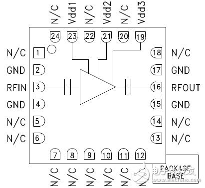
Figure 2: The HMC519LC4TR GaAs LNA provides low-noise gain for low-level inputs from 18 to 31 GHz; most package connections are used for power rails, ground, or are not used. (Image source: Analog Devices)
A design process is required, ranging from a simple functional block diagram to multiple external capacitors with different values and types, to provide appropriate RF bypassing and low parasitic effects on the three power rails, designated as Vdd (Figure 3).
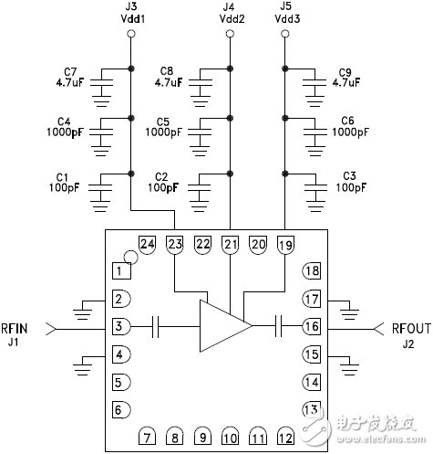
Figure 3: In practical applications, the HMC519LC4TR LNA requires multiple bypass capacitors with the same rated voltage on its power rails to provide large capacitance for low-frequency filtering and smaller-value capacitors for RF bypassing, thereby minimizing RF parasitic effects. (Image source: Analog Devices)
An evaluation board is generated based on this enhanced schematic, with detailed layout and BOM, including the use of non-FR4 printed circuit board materials (Figure 4(a) and 4(b)).
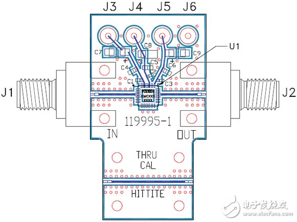
图4(a)
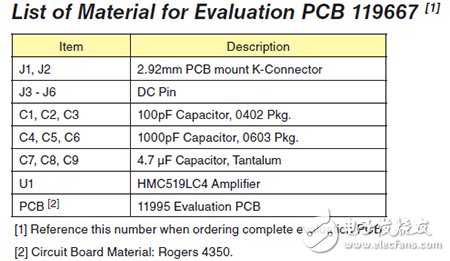
Figure 4(b)
Figure 4: Considering the high frequencies at which these LNA front-ends operate and the low-level signals they must capture, a detailed and tested evaluation design is crucial. This includes a schematic (not shown), circuit board layout (a), and BOM, as well as details of the passive components and printed circuit board materials (b). (Image source: Analog Devices)
The MACOM MAAL-011111 is a GaAs LNA for higher frequencies, supporting operation from 22 to 38 GHz (Figure 5). The device offers 19 dB of small-signal gain and a noise figure of 2.5 dB. While this LNA appears to be a single-stage device on the surface, it actually has three cascaded stages internally. The first stage is optimized for minimum noise and moderate gain, with subsequent stages providing additional gain.
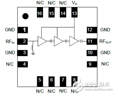
Figure 5: For users, the MAAL-011111 LNA appears as a single-stage amplifier, but it uses a series of gain stages internally, aimed at maximizing the signal-to-noise ratio (SNR) from input to output signal path while adding significant gain at the output. (Image source: MACOM)
Similar to Analog Devices' LNA, the MAAL-011111 requires only a low-voltage supply and is extremely compact at just 3×3 mm. Users can adjust and trade off certain performance specifications by setting the bias (supply) voltage to different values between 3.0 and 3.6 V. The recommended circuit board layout shows key printed circuit board copper dimensions needed to maintain proper impedance matching and ground plane performance (Figure 6).
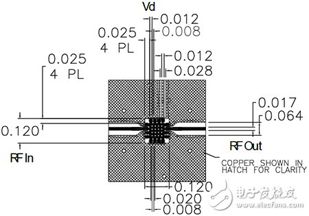
Figure 6: The recommended layout, making full use of MACOM's MAAL-011111, while providing input and output impedance matching. Note the use of printed circuit board copper (dimensions in millimeters) for impedance-controlled transmission lines and low-impedance ground planes. (Image source: MACOM)
PA Driving the Antenna
Contrary to the LNA's challenging signal capture, the PA takes relatively strong signals from the circuit with a high SNR and must be used to boost the signal power. All common factors related to the signal are known, such as amplitude, modulation, waveform, duty cycle, etc. This is the known signal/known noise quadrant in the signal processing diagram, which is the easiest to deal with.
The main parameter of the PA is the power output at the relevant frequency, with typical gain between +10 and +30 dB. Efficiency is another key parameter of the PA, second only to gain, but models of use, modulation, duty cycle, allowable distortion, and other aspects of the driven signal complicate any efficiency assessment. PA efficiency ranges from 30 to 80%, but this is largely determined by a variety of factors. Linearity is also a key parameter for the PA, judged by the IP3 value, just like in the LNA.
While many PAs use low-power CMOS technology (up to about 1 to 5 W), other technologies have matured and been widely applied in recent years, especially at higher power levels where efficiency is considered a key indicator of battery life and heat dissipation. In cases requiring several watts or higher power, PAs using gallium nitride (GaN) offer better efficiency at higher power and frequencies (typically 1 GHz). Especially considering efficiency and power dissipation, GaN PAs are highly cost-competitive.
The Cree/Wolfspeed CGHV14800F (1200 to 1400 MHz, 800 W device) is one of the latest representatives of GaN-based PAs. This HEMT PA's combination of efficiency, gain, and bandwidth is optimized for pulsed L-band radar amplifiers, enabling designers to find many applications in air traffic control (ATC), weather, anti-missile, and target tracking systems. Using a 50 V supply, it provides typical energy conversion efficiency of 50% and higher, and comes in a 10×20 mm ceramic package with a metal flange for cooling (Figure 7).
Figure 7: (Image source: Cree/Wolfspeed)

Figure 7: The CGHV14800F, a 1200 to 1400 MHz, 800 W GaN PA with a 10×20 mm ceramic package featuring a metal flange, must meet challenging RF and thermal requirements. Note that for mechanical and thermal integrity, the package is screwed (not soldered) to the printed circuit board when mounting the flange. (Image source: Cree/Wolfspeed)
The CGHV14800F is powered by a 50 V supply and typically offers 14 dB of power gain with an energy conversion efficiency of >65%. As with the LNA, evaluation circuits and reference designs are crucial (Figure 8).

Figure 8: In addition to the device itself, the demonstration circuit for the CGHV14800F PA requires very few components, but physical layout and thermal considerations are critical; considering installation integrity and thermal targets, the PA is fixed to the board via the package flange with screws and nuts (on the bottom, not visible). (Image source: Cree/Wolfspeed)
Also of great importance in many datasheets and performance curves is the power derating curve (Figure 9). This curve shows the relationship between available power output rating and case temperature, indicating that the maximum allowable power is constant at 115°C and then linearly decreases to the maximum rating at 150°C.
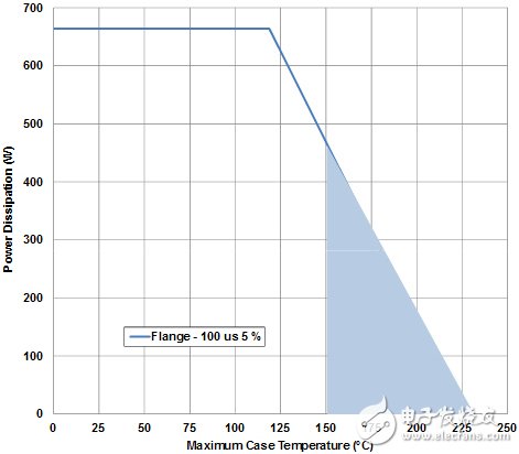
Figure 9: Because of its role in delivering power, the PA derating curve is needed to show designers how allowable output power decreases with increasing case temperature. Here, the rated power drops sharply after 115⁰C. (Image source: Cree/Wolfspeed)
MACOM also offers GaN-based PAs, such as the NPT1007 GaN transistor (Figure 10). Its frequency span from DC to 1200 MHz is suitable for both broadband and narrowband RF applications. The device typically operates from a single supply between 14 and 28 V and can provide 18 dB of small-signal gain at 900 MHz. The design is intended to withstand a 10:1 SWR (standing wave ratio) mismatch without device degradation.

Figure 10: MACOM's NPT1007 GaN PA spans from DC to 1200 MHz, suitable for both broadband and narrowband RF applications. Designers are also supported by various load-pull charts. (Image source: MACOM)
In addition to charts showing performance at 500, 900, and 1200 MHz, the NPT1007 also supports various "load-pull" charts to assist circuit and system designers striving to ensure stable products (Figure 11). Load-pull testing is performed using a pair of signal sources and signal analyzers (spectrum analyzers, power meters, or vector receivers).
The test requires observing the impedance variations of the device under test (DUT) to evaluate the PA's performance (including factors such as output power, gain, and efficiency), as all relevant component values may change due to temperature variations or tolerances around their nominal values.
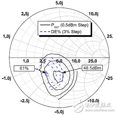
Figure 11: The load-pull chart for the NPT1007 PA goes beyond the minimum/maximum/typical specification standard table to show PA performance when its load impedance deviates from its nominal value (initial production tolerances and thermal drift can cause this in actual use). (Image source: MACOM)
Regardless of the PA process used, the output impedance of the device must be fully characterized by the supplier so that designers can properly match the device to the antenna to achieve maximum power transfer and maintain SWR consistency. The matching circuit is mainly composed of capacitors and inductors and can be implemented as discrete components or manufactured as part of the printed circuit board or even the product package. Its design must also sustain the PA power level. Once again, the use of tools such as the Smith chart is key to understanding and performing the necessary impedance matching.
Given the small chip size and high power levels of PAs, packaging is a key issue for PAs. As mentioned earlier, many PAs dissipate heat through wide thermal package leads and flange supports, as well as heat sinks under the package, as a path to the printed circuit board copper. At higher power levels (above about 5 to 10 W), PAs can have copper caps that allow heat sinks to be mounted on top and may require fans or other advanced cooling technologies.
The high power ratings and small size associated with GaN PAs mean that thermal environment modeling is crucial. Of course, it is not enough to keep the PA itself within allowable or junction temperature ranges. The heat dissipated from the PA must not cause problems for other parts of the circuit and system. The entire thermal path must be considered and addressed.
Summary
RF-based systems, from smartphones to VSAT terminals and phased array radar systems, are pushing the limits of LNA and PA performance. This has led device manufacturers to explore beyond silicon to GaAs and GaN to deliver the required performance.
These new process technologies offer designers devices with wider bandwidth, smaller packaging, and higher energy efficiency. However, designers need to understand the basics of LNA and PA operation to effectively apply these new technologies.